Background
Scatterometry-based metrology has the capability to perform high-throughput inspection of geometric characteristics of large-area nanopatterned surfaces. It utilizes physics-based dependencies between reflectance of light scattered from nanopatterned surfaces for pre-defined set of wavelengths and Critical Dimensions (CDs) of such nanopatterns.
Current practice necessitates existence of an a priori generated reference library of “reflectance spectra” to be simulated for an exhaustive set of possible underlying CDs characterizing the measured nanopatterns. Generating this library with resolution sufficiently high to result in adequate accuracy of the inferred CDs is time-consuming and can be infeasible, even for slightly complex nanopatterns.
Technical description
Researchers at The University of Texas at Austin have invented a method and process for optical inspection of CDs of complex nanopatterned surfaces. This process enables rapid and accurate inference of underlying CDs from reflectance spectra using a machine learning (ML)-based inverse problem realization. The inspection process is further accelerated with the optimized down-selection of spectral wavelengths involved in the inspection process.
Features
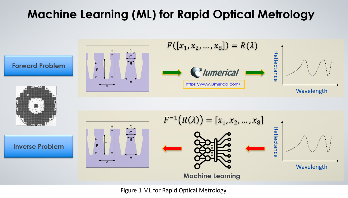
- Use of simulations, done using commercially available software, to generate a reference library of reflectance spectra expected from the corresponding nanopatterned surface to train a ML model using CDs and spectra for the ML-based realization of the inverse problem. See Figure 1.
- Use of a ML method which takes reflectance spectra gathered by the inspection devices as inputs, based on which it rapidly generates an output which estimates CDs characterizing the inspected pattern.
- Use of feature down-selection method to strategically choose wavelengths in the reflectance spectra which are the most informative about the underlying CDs, thus reducing the number of inputs for the ML model and further accelerating both the training and usage of the ML model.
Benefits
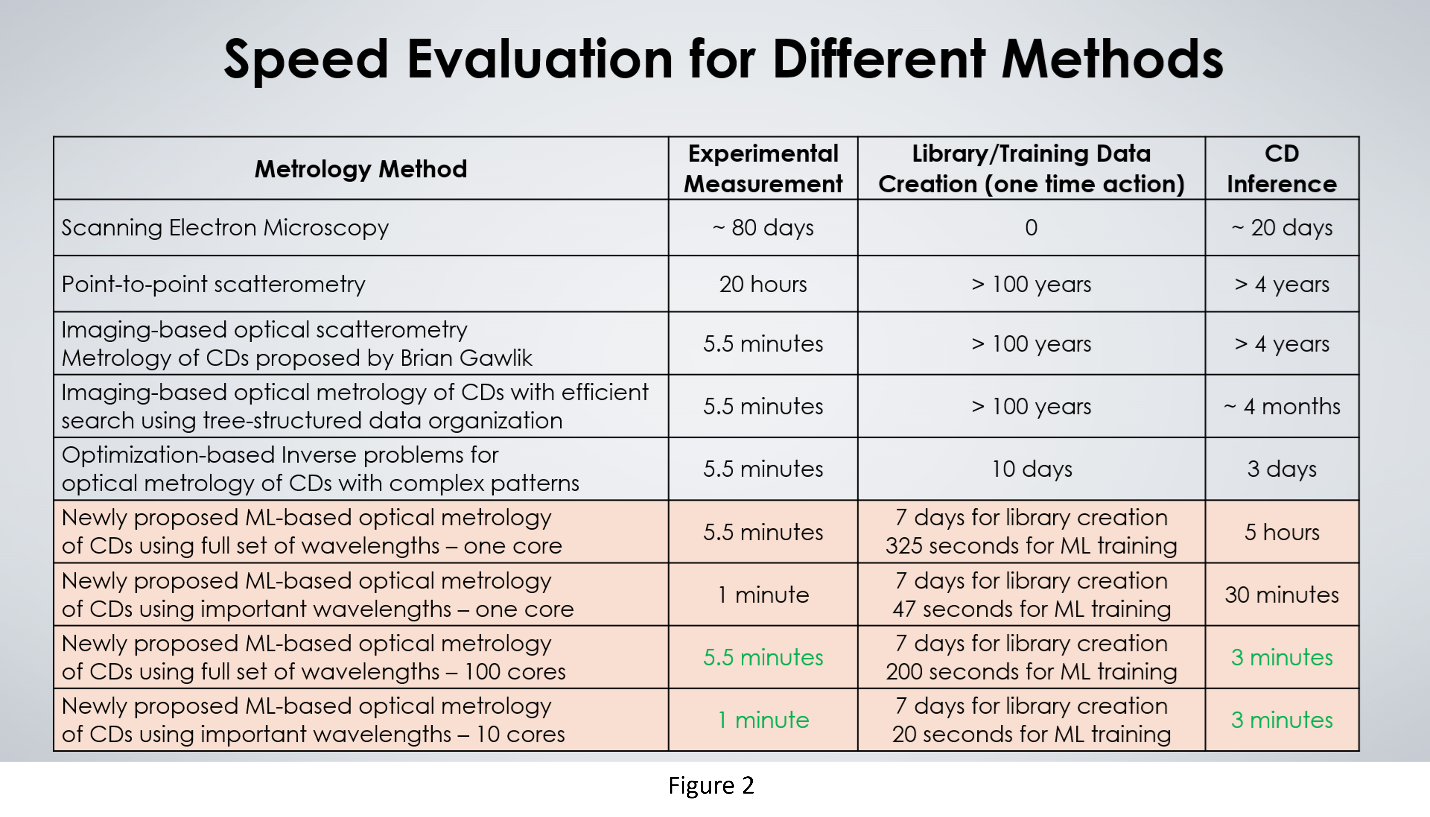
- The method enables order of magnitude faster measurement of geometries of nanopatterns compared to current best methods available. See Figure 2.
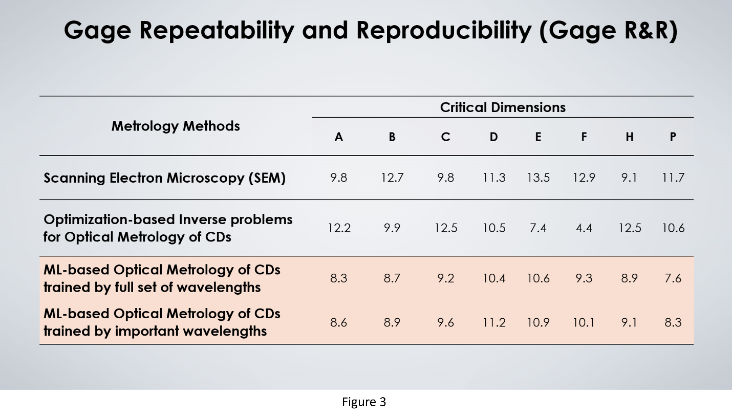
- Maintains the inspection accuracy and Gage Reproducibility and Repeatability (Gage R&R) comparable to most accurate microscopy methods. See Figure 3.
- The method has the potential to enable full inspection of a 300mm wafer with a nanopattern on it, as well as determination of the CDs across the entire wafer, all within minutes.
- The inspection time-scale is within the cycle times of the underlying processes (etch, deposition) and should enable immediate wafer-to-wafer control of those processes, as well as immediate detection of defects in the nanopatterns.


