Background
MicroLED technology are the next big display technology delivering stunning picture quality with spectacularly high resolution and brightness. MicroLED brings all the great aspects of OLED technology—self-emissive, perfect blacks, outstanding color, perfect off-angle viewing—while ditching the organic compounds to produce exceedingly thin panels. The major TV display OEMs have been actively showcasing huge displays, greater than 100-inch, at the yearly consumer electronics shows over the past few years to give us a taste of what’s to come for the home and consumer markets, as the technology remains very expensive to produce. At CES 2023, one TV display OEM unveiled a 76-inch version of its MicroLED display, making it the smallest-ever MicroLED people will be able to buy—albeit with a price tag of over $50,000.
MicroLED technology will also play a big role in AR/VR/mixed reality applications. Mixed reality headset applications, with short distances between the human eye and the display, dictate the need for displays to increase resolution to greater than 1,000 PPI. Atop of the desirable qualities of LEDs as a self-emissive illumination source, further size reduction to microLEDs allows for a larger number of devices (and hence pixels) in a fixed area. From a production standpoint, the impetus for device scaling to microLEDs is to increase the number of chips per wafer to reduce the cost of microLEDs in a bill of materials. As an example, in lower PPI applications such as next-generation high resolution displays for television, the microLED device dimension must be reduced to less than 10 µm for cost effectiveness.
From a production standpoint, the microLED display industry faces the problem of mass transfer. The manufacture of any microLED display involves making microLEDs—with diameters ranging from 5µm to 100µm—and using millions of these devices to form the self-emitting sub-pixels within a display. The traditional pick-and-place transfer process, assembling one sub-pixel at a time onto the display backplane, is no longer cost- and time-effective. While microLED display players have been devising alternative “mass transfer” processes (elastomer stamps or lasers to lift thousands of microLED chips from the source wafer to the display panel in a single swoop), as well as innovative transfer processes such as “fluidic assembly,” the basic manufacturing of microLED devices, shrinking to dimensions less than 10um, has led to significant yield issues at the production level. Most industry players form microLED structures by depositing 2D planar gallium nitride semiconductor layers on relatively small 100mm and 150mm sapphire substrates with advancements by companies growing nanowires directly on 200mm and 300mm silicon wafers. Currently, III-nitride heterojunction structures in devices require the use of plasma-based reactive ion etching (RIE) to etch and form LED devices (mesas/structures) on a larger substrate that is pre-produced with all the required semiconductor material layers. The use of RIE processes are detrimental to LED device efficiency, primarily via device sidewall damage, and increasingly so when shrinking LED devices into microLED devices.
This invention from researchers at The University of Texas and University of Illinois at Urbana-Champaign is a new processing method utilizing metal-assisted chemical etching, MacEtch (an anisotropic wet chemical etching technique), in combination with photo-illumination for relevant III-N heterojunction structures and materials utilized in conventional nitride-based LED devices. UT Austin’s partner institution UIUC has a suite of broader MacEtch IP available for license.
Technical description
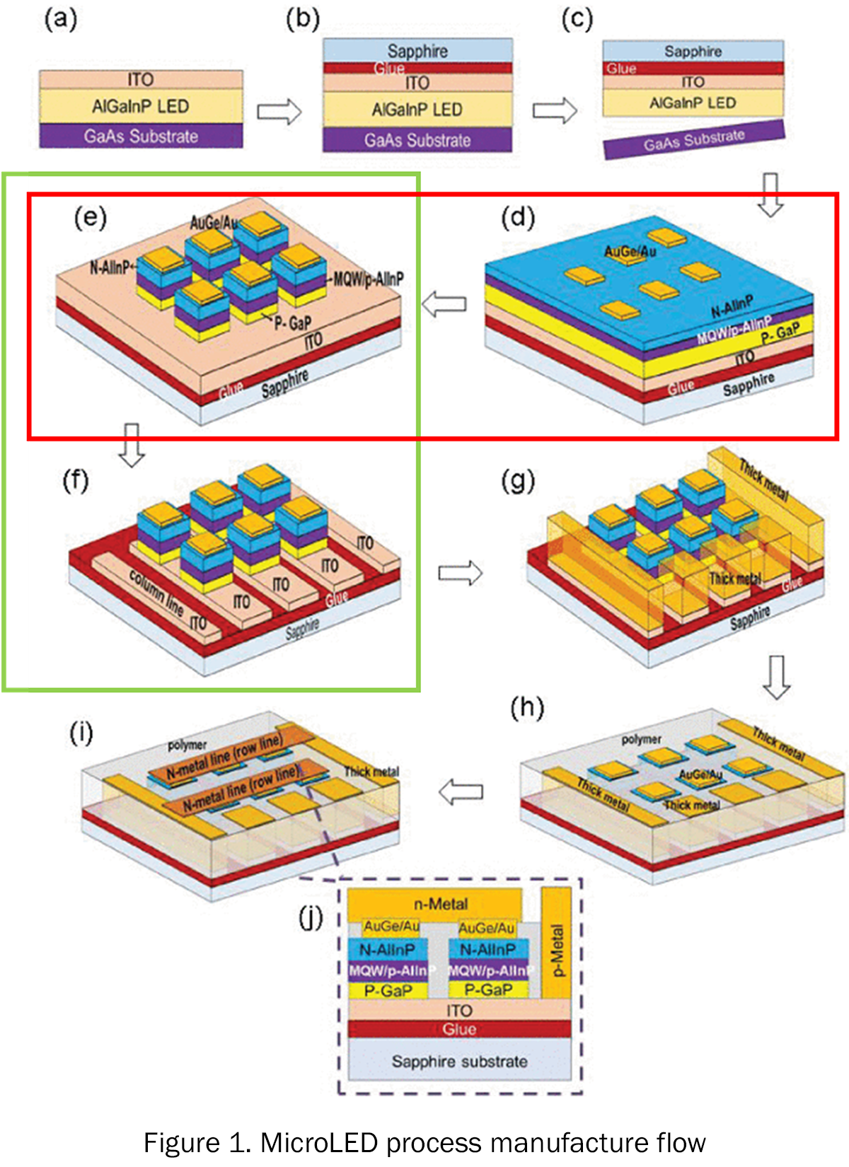
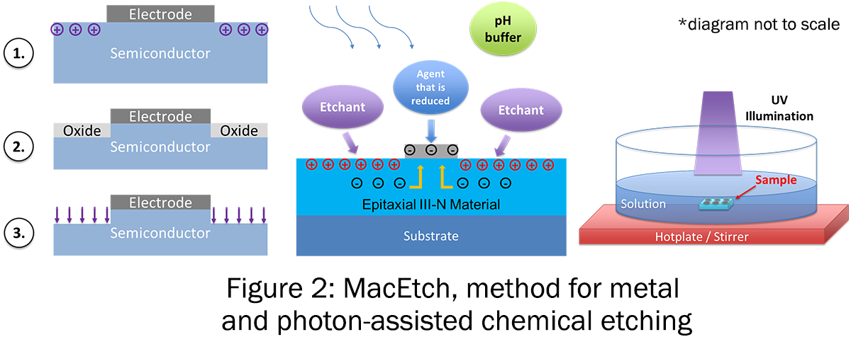
Figure 1 below shows a typical process flow for the manufacture of a MicroLED. Regardless of the material (III-N device not shown), the transition steps from (d) to (e) are universal and the state of the art utilizes RIE to convert a bulk, flat multi-layered structure into individual LED devices. This invention proposes to remove the steps highlighted by the red box. Not shown, in the process steps between (e) and (f) indicated by the green box, are typically treatment steps that need to be incorporated to “heal” or attempt to remove plasma damage incurred in the transition boxed in red. By utilizing this invention, MacEtch, we can ensure that the green boxed step has as little (or no) additional steps as possible which can reduce cost and increase throughput. A basic overview of how the etching method functions on single layer materials is shown in Figure 2 below.
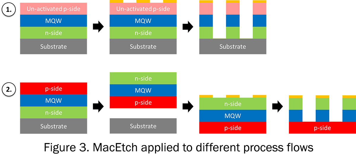
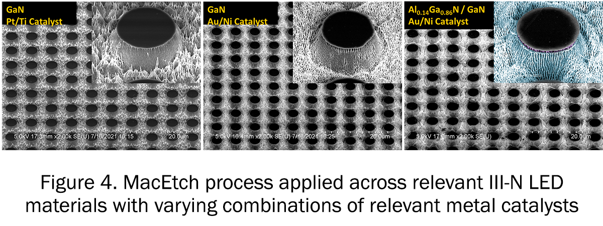
Figure 3 below shows how this invention can be applied to different microLED manufacturing process flows. Finally, Figure 4 below shows actual evidence that our etching process applies to relevant III-N LED materials, i.e. AlGaN, GaN and InGaN, with varying combinations of relevant metal catalysts that are typical of device contact metals as well (Pt, Ti, Au, Ni).
Benefits
- Production of sidewall damage-free micro and nanoscale heterojunction structures
- Compatibility with commercially grown device structures
- Pattern-able by industry CMOS-compatible methods
- Utilization of commercial device-compatible metal catalyst(s)
- Reduce cost and increase microLED yields at the wafer level