Background
Photoelectrochemical (PEC) water splitting is a promising technology for converting solar energy into clean and storable chemical energy. In PEC cells, semiconductors play a key role in absorbing photons from the light source to create mobile charge carriers. Various semiconductor materials have been studied for the high-performance PEC cells, including metal oxides, nitrides, Si, III-V compound semiconductor materials, and others. Among these, Si-based photoelectrodes have attracted substantial interest due to silicon’s moderate bandgap (1.12 eV), high charge mobility and diffusion lengths, and well-established technological infrastructure.
However, Si-based photoanodes for the oxygen evolution reaction (OER) remain challenging to engineer, due to the complex four-electron reaction mechanism which requires a large overpotential, and low chemical stability in alkaline solutions. To improve the OER performance of Si-based photoanodes, metal-insulator-semiconductor (MIS) structures have been widely used for Si-based photoanodes, due to their high efficiency and good stability. An efficient metal catalyst at the surface can improve the reaction kinetics of photoanodes, reducing the overpotential for OER. Corrosion of Si in aqueous electrolytes can be prevented in MIS photoelectrode structures by protecting the Si surface with thin layers of insulators.
Technology description
Researchers at The University of Texas at Austin have demonstrated a low cost and highly scalable method for improving Si-based MIS photoanodes by exploiting a thin-film reaction of Al through an insulating oxide layer followed by Ni‑electrodeposition, and not requiring any lithographic patterning. The thin-film reaction of Al with SiO2 or Si, leading to localized penetration of Al “spikes” into the underlying material, has been studied extensively since it can cause an electrical short in silicon pn-junction structures with Al contact metallization. Al spiking can also occur through an insulating SiO2 layer, and has been exploited to form Ohmic contacts through an oxide passivation layer on Si. In an MIS photoelectrode structure with Al as the metal layer, annealing of the Al/SiO2/Si structure above 300°C causes Al to penetrate the underlying SiO2 and induces formation of localized metal spikes in the MIS structure.
Results
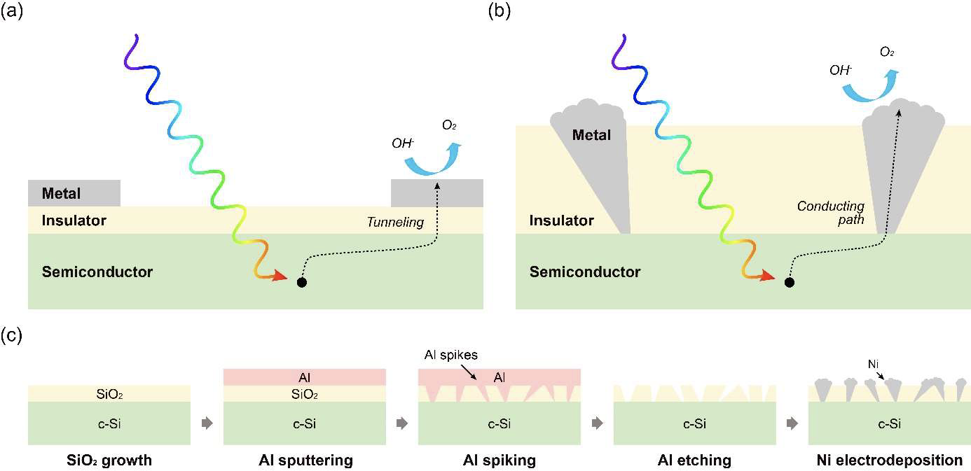
Figure 1. Schematics of metal-insulator-semiconductor photoanodes. Images a) and b): Schematics of MIS photoanodes for OER process by tunneling through a thin insulator (a) and passing along the conductive path through the localized metal spike (b). Image c): Schematic of the fabrication methods for the spiked Ni/SiO2 /Si MIS photoanode structure.
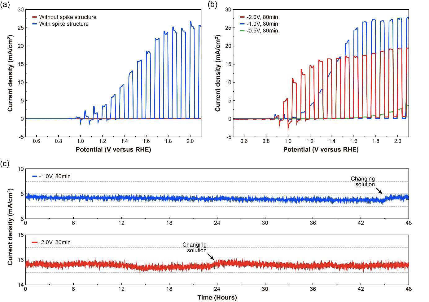
Figure 2. PEC characterization for the Ni/SiO2 /n-Si photoanodes. Image a) LSV curves with chopped illumination in 1M KOH solutions for the Ni/SiO2 /Si photoanodes with and without spike structure caused by Al spiking, b) LSV of Ni/SiO2 /Si photoanodes with spike structures for different Ni electrodepositions at -0.5, -1.0, and -2.0 V of applied biases, and c) 48 hours of CA stability tests at -1.3 V versus RHE in 1M KOH solutions for spiked Ni/SiO2 /Si photoanodes with 80 min Ni electrodepositions at -1.0 and -2.0 V.