Through silicon vias (TSV) is a key enabling element the provides short vertical interconnects in die stacks to improve electrical performance, power consumption, and form factor for 3D integrated devices. The mismatch of thermal expansion coefficients between the copper via and the silicon wafer can induce significant thermal stresses to degrade the device performance and induce structural failure, raising serious reliability concerns. Of particular concern is the extrusion induced by thermal stresses at the top of the copper via, which can damage the TSV and the adjacent interconnected structures. This has been identified as a critical yield and reliability problem in the manufacturing and operation of 3D integrated circuits.
Technology description
Researchers at The University of Texas at Austin have identified a solution by applying a cap layer which constitutes a thin metallic layer which can react with the copper TSV underneath to form an alloying layer at the interface or partly dissolve into the copper grain boundaries. This will reduce the interfacial and grain boundary mass transport and thus decrease the amount of TSV extrusion. The candidate metals include Co, Ti, Ni, Al, and their compounds, such as NiAl.
Results
A 16nm thin film of Co was deposited onto the top surface of the TSV. Results showed that the addition of the cap layer decreased via extrusion, as well as the mass transport responsible for stress relaxation.
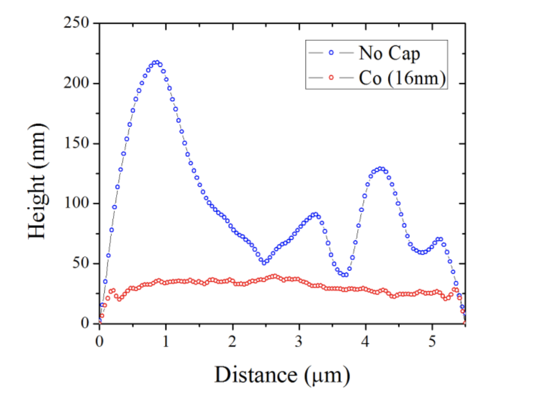
Figure 1: AFM scan of via extrusions with and without the Co cap layer.
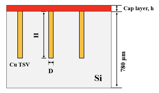
Figure 2: Schematic of experimental design using a cap layer.