Background
The development of accurate surface imaging is key to implementing an effective metrology strategy to manage defect detection in high volume electronic device fabrication. Measurement of manufacturing processes can be performed either in-line, as part of the manufacturing process, or off-line in a separate process. Unfortunately, no methods currently exist to interrogate nanoscale features in-line with high-rate nanomanufacturing processes.
Technology description
Researchers at The University of Texas at Austin have demonstrated a metrology device, which uses AFM probes to be integrated directly into the fabrication lines. This technology consist of a compound, double parallelogram flexure-hinge mechanism (DPFM) based nanopositioning system with stacked coarse-fine adjustment DPFMs. Almost all current probe based measurement instruments, such as AFMs, measure the deflection of the probe tip with a laser interferometer based instrument. While extremely accurate, this method is not compact and requires a significant amount of specialized and bulky equipment which does not allow for in-line measurement. In concert with novel Atomic Force Microscope (AFM)–on-a-chip technology, this coupled, multi-flexure positioning system is proposed as a probe-based metrology device for wafer or roll-to-roll (R2R) manufacturing.
Results
There are many studies of double parallelogram flexure mechanisms (DPFM), which demonstrate extreme precision with mm-scale displacement range. It is possible to package, in a compact fashion, multiple AFM probes over a single substrate in a single precisely positioned structure. The number of probes that can be arrayed is only limited by the width of the sample to be measured and the length of the surface on which the sample is measured. Thus, the throughput of the device is highly expandable at a relatively small incremental cost. This enables measurement, evaluation, or processing of an area orders of magnitude larger than any direct measurement currently available. Additional details may be found here and here.
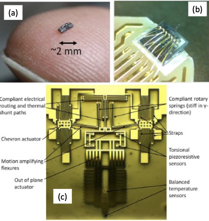
Figure 1. (a) A single AFM Chip, (b) packaged instrument, and (c) layout of MEMS chip
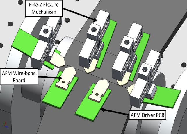
Figure 2. Individual AFM positioned array layout