Background
A majority of power devices are Si MOSFET or IGBT. Wide band gap (WBG) material based devices are posed to replace Si MOSFET and IGBT in the future. Silicon Carbide (SiC) and Gallium Nitride (GaN) are the two most matured materials, with SiC considered the more promising of the two. Today, SiC power MOSFET is made vertically; GaN is made laterally. SiC devices are very suitable for high voltage application, while GaN devices are very suitable for high frequency application with a breakdown voltage less than 600V. Because of this and several other factors, GaN FET is faster than SiC and can be used in high frequency application. There is no SiC lateral power device on the market that can compete with GaN. This invention is a family of SiC lateral power devices that can compete with GaN.
Technology description
Researchers at The University of Texas at Austin have developed a family of lateral power switches on SiC substrate that are easy to fabricate and will offer superior performance to GaN FET. It is also suitable for developing SiC power integrated circuits. In addition to power electronics application (used as switches with frequency from KHz to MHz), the proposed switches can also be used in amplifier applications such as RF amplifiers.
- Easy to fabricate
- Lower RDSon
- Lower capacitance
- Suitable for integrating multiple devices and drivers together
Benefits
- Energy efficiency: Better device performance, enabling higher efficiency in power supplies
- High density: Enables higher frequency application to reduce passive component size
- Single chip integration: Results in further power density improvement

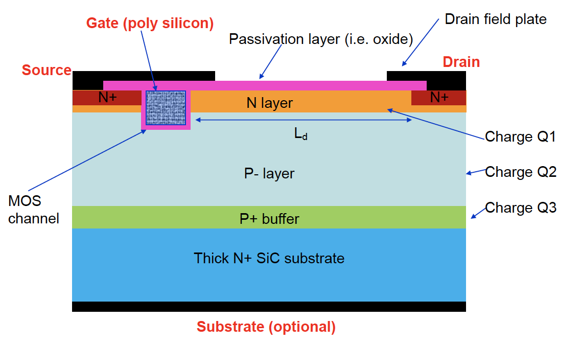
Figure 1: A single embodiment of a Lateral MOSFET on SiC.

