Background
Strained layer superlattices (SLSs) have attracted significant attention as potential light absorbers for infrared (IR) photodetector applications. Such semiconductor-based structures provide effective band gaps across mid-wave to long-wave IR that are tunable by control of layer thicknesses and material composition. Of particular interest is the predicted improved performance of SLS-based detectors in the key metrics of both dark current and fabrication costs when compared to the current state-of-the-art HgCdTe photodetectors.
Technology description
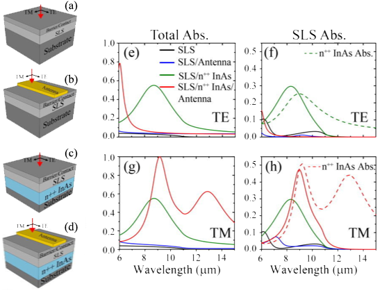
Researchers at The University of Texas at Austin have demonstrated a detector architecture for enhanced absorption based on nanoscale SLS layers. The architecture relies on the ability to control the complex reflection coefficient at the interface between an n++ InAs layer and the SLS layer. This allows for the strong confinement of incident light in an ultra-thin a-SLS layer. A metal antenna is added on the top of the device to allow for further control of the optical properties of the detectors. This structure gives near perfect total absorption and additional absorption enhancement in the a-SLS layer.
Results
Using the proposed design, researchers demonstrated the potential for near 50% detector absorption in ~100-200nm thick a-SLS layers. They also were able to tune the absorption resonance by altering the geometry with little to no degradation in the a-SLS absorption. This patent pending device architecture offers the potential for strong polarization-selectivity, ultra-thin, high efficiency detectors with minimized growth costs and relaxed design parameters. In the image below (a)–(d) Schematics of the four detector architectures investigated. TE-polarized (e) total and (f) a-SLS and TM-polarized (g) total and (h) a-SLS absorption for each of the four architectures. Absorption in the n++ groundplane for the structures in (c) and (d) is shown as dashed lines in (f) and (g). Additional details may be found in this published article.


