Background
The explosion of global data rates has led to an increased reliance on optical transceiver technologies for high-throughput data centers and high-performance computing. Photonic integrated circuits improve the performance of optical technologies and reduce their cost.
Many key elements in photonic integrated circuits, such as modulators and switches, require the presence of some sort of electro-optic effect to map electrical and optical signals onto one another, thereby converting electronic data into optical data. Many physical mechanisms can be exploited to produce an electro-optic effect, but one of the most efficient in terms of speed and power consumption is the Pockels effect. BaTiO3 (BTO) has a large Pockels effect and can be integrated on silicon substrates, making it an ideal material for use in next-generation photonic integrated circuits. Attempts to exploit the BTO in photonic integrated circuits rely on designs that incorporate other materials, such as silicon or silicon nitride, into the waveguides rather than designing waveguides from BTO. These hybrid BTO waveguides suffer from reduced performance relative to pure BTO waveguides due to a decreased optical power confinement in the BTO.
Our invention of monolithic, unetched BTO strip waveguides better harnesses the benefits of BTO as an electro-optic material without the need for integrating other materials with the waveguides or etching the BTO, which can lead to unacceptable optical propagation losses.
Technology description
Researchers at The University of Texas at Austin have developed a portfolio of technologies to enable the use of BTO material into photonic devices. The first invention comprises a BTO strip waveguide integrated on silicon substrates without the incorporation of other materials into the waveguide that would limit operating efficiency.
The second invention is a method for creating strained a-axis oriented BaTiO3 films on silicon for electro-optic and other applications requiring in-plane ferroelectric polarization by using a stannate perovskite buffer layer, in addition to the normal SrTiO3 buffer layer required to grow any pervoskite oxide on silicon.
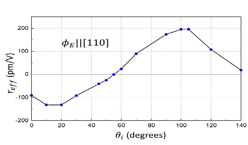
Finally, the researchers have demonstrated a dynamic waveguide from barium titanate thin films by utilizing the Pockels effect in barium titanate to dynamically create index contrast in the film via an externally applied electric field. A Pockels coefficient of 923 pm/V, which is 30 times larger than lithium niobate devices
Results
Demonstration of the Pockels effect of BTO devices grown on Si and Ge substrates. Detailed description of the studies may be found in the following publications:
 |  |
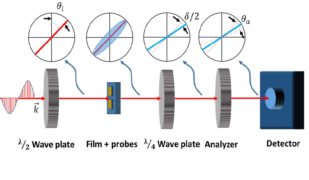
Schematic of the electro-optic measurement
setup used | Effective Pockels coefficient of the film versus the rotation of the input polarization angle |


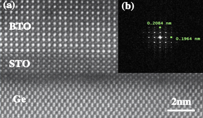
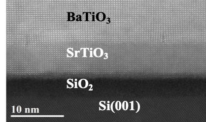
SEM images of the layers

