Background
Two technologies are touched upon. First is an energy-efficient comparator, followed by a time domain two-step capacitance-to-digital converter.
Comparators bridge the analog and digital world. A low-power, low-noise comparator is critical for analog-to-digital converters. A comparator consists of a pre-amp followed by a latch. Dynamic comparators, such as Strong-Arm (SA) latch-based comparators, use dynamic integrators instead of static pre-amps to remove static current and reduce power consumption. A conventional dynamic integrator based pre-amp has several limitations: no current reuse, full discharge of load capacitors, strong performance dependence on the input common-mode (CM) voltage, and low effective pre-amp gain.
Capacitive sensors are widely used to measure various physical quantities, including pressure, humidity, and displacement. Ultra-low-power capacitance-to-digital converters (CDCs) are required for sensors with limited battery capacity or powered by energy harvesters. A SAR CDC is simple to design and well-suited for low-to-medium resolution applications. However, to reach high resolution, it requires a low-noise comparator or OTA-based active charge transfer, resulting in degraded power efficiency.
Results
Researchers at The University of Texas at Austin have developed a dynamic comparator that addresses these issues by introducing a floating inverter amplifier (FIA) based pre-amp. This pre-amp uses an inverter-based input pair powered by a floating reservoir capacitor. The inverter based input stage allows for current reuse while the floating reservoir capacitor prevents full discharge of the load capacitor and makes the pre-amp operation less sensitive to input CM variation. This design also increases potential pre-amp gain by removing a major limitation caused by the output CM drop. The prototype proved this solution to be highly efficient and robust. Manufactured in 180nm, it is the most energy-efficient published design currently with >7× improvement in energy efficiency compared to a standard SA latch and and >2.5× improvement over the second-best published design. It is also the only dynamic comparator with common-mode rejection and process corner insensitivity, which provides robustness against environmental interference.
Additionally, researchers have developed an incremental two-step CDC with a time-domain ΔΣM (TDΔΣM) that achieves a resolution of 0.29fF while dissipating only 0.083nJ per conversion, which improves the energy efficiency by >2× compared to the state-of- the-art CDCs. This is achieved by performing ΔΣ modulation in the time domain. The prototype CDC was fabricated in 40nm CMOS with a 20fF SAR unit capacitor and 10fF TDΔΣM unit capacitor. It occupies an area of 0.06 mm2. Additional details may be found here and here.
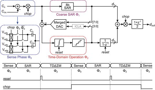
Figure 1. CDC layout
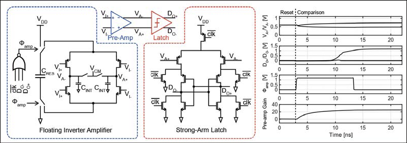
Figure 2. Full dynamic comparator.